Author Affiliations
Abstract
1 Beijing National Research Center for Information Science and Technology (BNRist), Department of Electronic Engineering, Tsinghua University, Beijing 100084, China
2 China Mobile Research Institute, Beijing 100053, China
3 MIIT Key Laboratory for Low-dimensional Quantum Structure and Devices, School of Materials Sciences & Engineering, Beijing Institute of Technology, Beijing 100081, China
With the swift advancement of neural networks and their expanding applications in many fields, optical neural networks have gradually become a feasible alternative to electrical neural networks due to their parallelism, high speed, low latency, and power consumption. Nonetheless, optical nonlinearity is hard to realize in free-space optics, which restricts the potential of the architecture. To harness the benefits of optical parallelism while ensuring compatibility with natural light scenes, it becomes essential to implement two-dimensional spatial nonlinearity within an incoherent light environment. Here, we demonstrate a lensless opto-electrical neural network that incorporates optical nonlinearity, capable of performing convolution calculations and achieving nonlinear activation via a quantum dot film, all without an external power supply. Through simulation and experiments, the proposed nonlinear system can enhance the accuracy of image classification tasks, yielding a maximum improvement of 5.88% over linear models. The scheme shows a facile implementation of passive incoherent two-dimensional nonlinearities, paving the way for the applications of multilayer incoherent optical neural networks in the future.
Photonics Research
2024, 12(4): 682
Author Affiliations
Abstract
1 Beijing Engineering Research Center of Mixed Reality and Advanced Display, School of Optics and Photonics, Beijing Institute of Technology Beijing, China
2 College of Optics and Photonics, University of Central Florida, Orlando, FL 32816, USA
3 MIIT Key Laboratory for Low-Dimensional Quantum Structure and Devices, School of Materials Science & Engineering, Beijing Institute of Technology Beijing, China
Since the invention of holography by Dennis Gabor, the fabrication of holograms has mainly relied on direct recording of wavefront by engraving the intensity fringes of interfering electric fields into the holographic material. The degree-of-freedom (DoF) is often limited, especially for its usage as a holographic optical element in imaging or display systems, as what is recorded is what to use. In this work, based on the emerging self-assembled photo-aligned liquid crystal, a polarization hologram with full DoF for local manipulation of optical structure is demonstrated. The ability to record an arbitrary wavefront (in-plane DoF) is achieved by freeform surface exposure, while the local adjustment of deposited liquid crystal (out-of-plane DoF) is realized by inkjet printing. The methodology for designing and fabricating such a hologram is exemplified by building a full-color retinal scanning display without color crosstalk. Here, the arbitrary wavefront modulation capability helps to eliminate the aberrations caused by mismatched exposure and display wavelengths. The local liquid crystal adjustment ability enables the suppression of crosstalk by variation of chiral pitch and film thickness to tune the peak and valley of Bragg diffraction band. The demonstrated method is expected to greatly impact the fields of advanced imaging and display, such as augmented reality and virtual reality, that require optics with an ultrathin form factor and high degrees of design freedom simultaneously.
1 北京理工大学材料学院低维量子结构与器件工信部重点实验室,北京 100081
2 北京理工大学物理学院纳米光子学与超精密光电系统北京市重点实验室,北京 100081
双激子发光是半导体材料在高激发强度下形成两个激子后复合发光的一种物理过程。相较于块体材料,量子点体积小、载流子受限、能级分立,从而具有独特的双激子发光特性,具体表现为双激子结合能大,级联发射中的光子对是极化反对称的,激子对的俄歇复合效应强。从双激子发光研究的发展历程出发,重点介绍了量子点双激子发光的基本原理、光谱特性,特别是量子效应对量子纠缠和光增益的影响。讨论了量子点双激子发光在纠缠光源、量子点激光器等方面的应用潜力和目前所面临的挑战。
量子光学 量子点 双激子 纠缠光子源 俄歇复合 光增益

Author Affiliations
Abstract
1 State Key Laboratory for Mesoscopic Physics and Frontiers Science Center for Nano-optoelectronics, School of Physics, Peking University, Beijing 100871, China
2 Collaborative Innovation Center of Extreme Optics, Shanxi University, Taiyuan 030006, China
3 MIIT Key Laboratory for Low-Dimensional Quantum Structure and Devices, School of Materials Sciences and Engineering, Beijing Institute of Technology, Beijing 100081, China
4 School of Science, RMIT University, Melbourne 3000, VIC, Australia
5 Peking University Yangtze Delta Institute of Optoelectronics, Nantong 226010, China
Perovskite-enabled optical devices have drawn intensive interest and have been considered promising candidates for integrated optoelectronic systems. As one of the important photonic functions, optical phase modulation previously was demonstrated with perovskite substrate and complex refractive index engineering with laser scribing. Here we report on the new scheme of achieving efficient phase modulation by combining detour phase design with 40 nm ultrathin perovskite films composed of nanosized crystalline particles. Phase modulation was realized by binary amplitude patterning, which significantly simplifies the fabrication process. Perovskite nanocrystal films exhibit significantly weak ion migration effects under femtosecond laser writing, resulting in smooth edges along the laser ablated area and high diffractive optical quality. Fabrication of a detour-phased perovskite ultrathin planar lens with a diameter of 150 μm using femtosecond laser scribing was experimentally demonstrated. A high-performance 3D focus was observed, and the fabrication showed a high tolerance with different laser writing powers. Furthermore, the high-quality imaging capability of perovskite ultrathin planar lenses with a suppressed background was also demonstrated.
Photonics Research
2022, 10(12): 2768
1 北京理工大学光电学院精密光电测试仪器及技术北京市重点实验室, 北京 100081
2 北京理工大学材料学院低维量子结构与器件工信部重点实验室, 北京 100081
3 北京理工大学深圳研究院, 深圳 518057
微透镜阵列是一种多功能的微光学元件,可以对入射光进行扩散、光束整形、光线均分、光学聚焦等调制,进而实现大视角、低像差、小畸变、高时间分辨率和无限景深等,在光电器件和光学系统的微型化、智能化和集成化方面具有重要的应用潜力。介绍了微透镜阵列的光学原理和发展历程,综述了喷墨打印、激光直写、丝网印刷、光刻技术、光聚合技术、热熔回流技术和化学气相沉积法等微透镜阵列制备技术,总结了微透镜阵列在成像传感、照明光源、显示和光伏等领域的应用进展,最后对微透镜阵列的发展方向进行了展望,讨论了曲面微透镜、叠加复眼系统以及微透镜与新型光电材料结合等新方向的发展趋势和未来挑战。
光学制造 微透镜阵列 制备技术 器件集成 光学系统 显示 光学学报
2021, 41(21): 2100001
Author Affiliations
Abstract
1 Beijing Key Laboratory of Nanophotonics and Ultrafine Optoelectronic Systems, Key Laboratory of Photoelectronic Imaging Technology and System, Ministry of Education, School of Optics and Photonics, Beijing Institute of Technology, Beijing 100081, China
2 Yunnan KIRO - CH Photonics Co., Ltd., Kunming 650223, China
3 School of Materials Science & Engineering, Beijing Institute of Technology, Beijing 100081, China
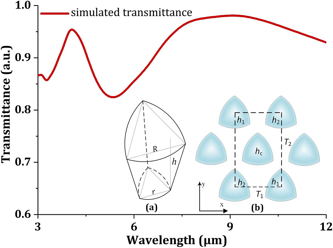
A gradient-index Reuleaux-triangle-shaped hole array was fabricated on germanium (Ge) by nanoimprint lithography and inductively coupled plasma processing as a broadband mid-infrared (IR) antireflective surface. The interaction between the {111} planes of cubic crystalline Ge and a circular mold successfully produced an orderly and periodically distributed Reuleaux-triangle-shaped hole array. As a result, the average transmittance increased 15.67% over the waveband at 3–12 μm and remained stable at the incidence angle of up to 60°. The vertices of the Reuleaux triangle showed local enhancement of the electric field intensities due to interference of the incident and reflected radiation fields. It was also found that nonuniform hole depths acted to modulate the transmittance over the 3–12 μm waveband.
240.6700 Surfaces 160.4670 Optical materials Chinese Optics Letters
2019, 17(12): 122401


